Product
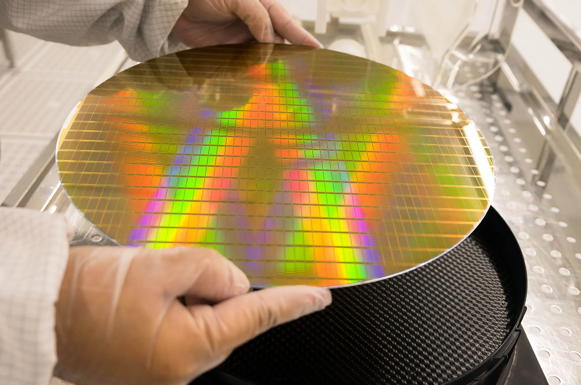
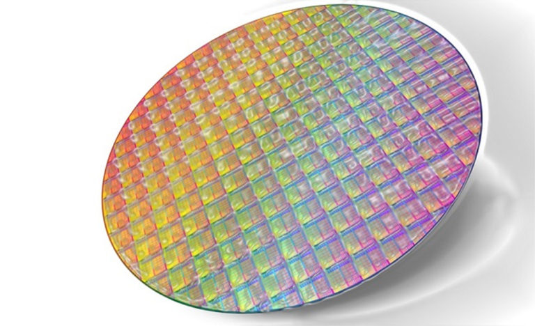
Silicon Wafers
Introduction
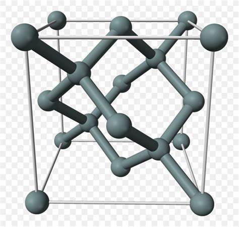
Silicon wafers are essential components in the semiconductor industry, serving as the foundational material for integrated circuits and microelectronics. These wafers are typically made from high-purity single-crystal silicon, and their precise properties are crucial for electronic device performance.
-
Preparation using traditional method
The traditional method for preparing silicon wafers involves a series of complex and resource-intensive steps. It begins with the purification of silicon, followed by the growth of large single-crystal ingots through the Czochralski or float-zone method. These ingots are then sliced into thin wafers and subjected to extensive chemical and mechanical processing to achieve the desired thickness, flatness, and surface quality.
-
Reaction
The primary chemical reactions in the traditional method involve the purification of silicon using the Siemens process or the reduction of silicon tetrachloride (SiCl4) with hydrogen gas to produce high-purity silicon. These reactions require high-temperature and energy-consuming processes, making them environmentally unfriendly.
-
Disadvantages of traditional method
The major disadvantage of the traditional method is its high energy consumption and environmental impact. It generates significant waste and emissions, contributing to pollution and resource depletion. Additionally, the process is time-consuming and costly, limiting its sustainability and scalability.
-
Preparation using Green method
In recent years, there has been a shift towards more sustainable and eco-friendly methods for preparing silicon wafers. Green methods focus on reducing energy consumption, waste, and environmental impact. One such approach involves recycling silicon scraps and using them as a source material for wafer production, minimizing the need for new silicon purification.
-
Reaction
The green method for silicon wafer preparation often involves the recycling of silicon wafers or scraps, which are melted down and processed into new wafers. This process significantly reduces the energy and resource requirements, making it a more sustainable alternative to traditional methods.
-
Advantages of Green method
The primary advantage of the green method is its reduced environmental impact and energy consumption. It contributes to resource conservation and waste reduction while lowering the overall production costs of silicon wafers. This approach aligns with the growing emphasis on sustainability in the semiconductor industry.
-
Applications
Silicon wafers, whether prepared using traditional or green methods, are integral to the manufacturing of various electronic devices. They are used in the fabrication of integrated circuits, microprocessors, memory chips, and sensors, among others. The continued development of sustainable and green methods for silicon wafer production is crucial for the long-term sustainability of the semiconductor industry and the electronics we rely on in our daily lives.